
1. 4nm FinFET: A Scalable Platform Built on Proven Maturity
Samsung Foundry’s 4nm FinFET process represents a well-balanced optimization of performance and stability. In semiconductor manufacturing, achieving both simultaneously remains a fundamental challenge: leading-edge nodes deliver higher performance but carry initial mass production risks, while mature nodes offer stability with limited performance headroom. The 4nm process is designed to effectively address this challenge.
Positioned at the boundary between leading-edge and mature technologies, the 4nm process leverages extensive mass production experience to ensure high yield and process stability. At the same time, it offers a wide range of design options that enable optimal implementation at this node. As a result, it simultaneously enhances performance, power efficiency, and design flexibility - providing customers with a practical and reliable solution that balances performance with manufacturability.
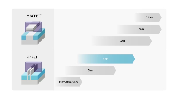
[Figure 1] 4nm Process in the Technology Roadmap
2. Expanding Process Options: Greater Flexibility in Transistors and Interconnects
Performance gains in the 4nm process are not driven by scaling alone, but by the co-optimization of both transistors and interconnects.
On the transistor side, a wide range of Threshold Voltage (Vth) options enables enhanced design flexibility. Ultra-low Vth (uLVT) devices improve switching speed and are well-suited for high-performance designs, while high Vth (HVT) devices reduce leakage current, improving standby power efficiency. In addition, combining uLVT devices with reduced operating voltage enables further dynamic power reduction. These options allow designers to fine-tune the balance between performance and power with greater precision.
Significant improvements have also been made in the interconnect stack. As scaling progresses, increasing resistance and capacitance in metal layers can limit signal propagation speed. To address this, the 4nm process introduces additional interconnect layers with relatively larger pitch and improved Resistance-Capacitance (RC) characteristics, achieving approximately a 26% reduction in RC delay. This improvement goes beyond raw speed enhancement, enabling more efficient data flow across the entire chip.